My Sega Star Trek Captain’s Chair is destined to be present at the 2012 Texas Pinball Festival. As a result; the game needs to have a FreePlay feature (IE a way for the public to play the game without needing quarters). I know Sega Star Trek has a freeplay rom hack available; however, at this moment, VectorLabs isn’t supplying freeplay roms with their devices. I haven’t spent enough time with the multi-vector boardset to determine how easy/hard it would be to convert to Freeplay. As a result; I wanted a simple inexpensive way to credit up the machine when the user pressed the Start button (1UP).
I toyed with the idea of using a cheap 8pin ATMEL microcontroller; but decided a simple 555 timer could be developed to do most of the heavy lifting. In the end I decided to go with a dual 555 timer (NE556) in a cascaded mono-stable configuration. The circuit features:
- PowerOn Reset to “credit up” a single credit when power is applied to the machine. Jumpered feature.
- Ability to drive COIN_NO signals
- Ability to “interrupt” COIN_NC
- Can be alternatively stuffed for AC power supplies (6.3VAC GI circuits in Pinball Coindoors).
- Jumper configuration to “disable” circuit.
- Barrier Diodes to help prevent “installation error”.
I have decided to release this design under to the public under the TAPR Non-Commercial Open Hardware License which indicates:
You may make products based upon this design, provided you do not make more than ten units in any twelve month period for your personal use.
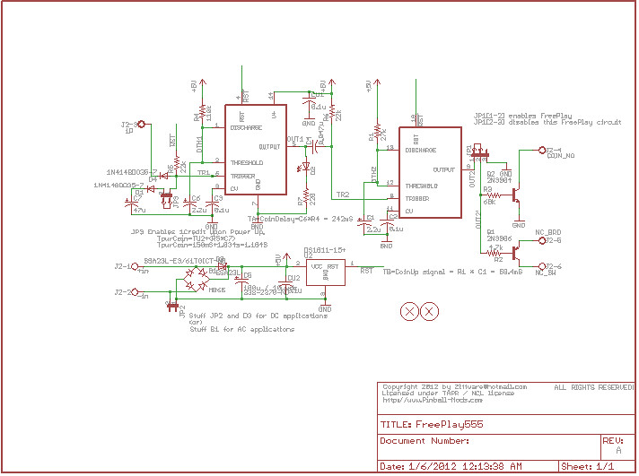
Schematics :
The first timer conditions the active low switch connected to J2-3 (1P [aka the start button]). On the Sega vector hardware; this signal is tied high to 5V via a 2.2K pullup resistor. The start button connects momentary grounds at this signal. The Trigger on the 555 timer is also triggered when the voltage at pin 6 transitions below 1/3VCC. D4 protects the cpu board by preventing current from flowing back into the cpu board. This timer “de-bounces” the switch which sends a single long pulse via OUT1 (pin 5). This timing is created by TA = C6*R4 or ~242mS. I’ll explain the function of R5, JP3, D1, and C7 later.
OUT1 drives the “armed” LED to notify the user/debugger that a “start” pulse was received. OUT1 is coupled to Timer2 via C4 and R6. The purpose of these components is to provide a “negative” trigger pulse at the falling edge of Output. Timer2 then drives based upon TB = R1*C1 or ~60mS. This is the coinup signal which is sent to the coin circuit of the arcade machine. 60mS was derived from measurements of my acutal Star Trek Captain’s Chair by dropping a quarter into the slot via an Oscope.
OUT2 (pin9) drives Q2 and Q1 respectively. When not processing “start/coin up signals” Q1 is “active” providing conduction between the CPU Board and the Switch (PNP active when base is low). On the sega star trek; I found that I had to interrupt the NC signal of the switch in the coin door to get the cpu to “detect” a coin from our COIN_NO (J2-4) – Q1 provides this interruption. Speaking of NO, Q2 goes active when OUT2 outputs a high… which drives a “low” to the COIN_NO. In the Vector machine; COIN_NO is pulled high thru another 2.2k resistor and drives the !Set signal of a Set/Reset Latch made out of NAND gates. Incidentally; the NC signal drives the !Reset signal. The Q output of the NAND gate drives the clock of a D latch which drives the interrupt pin to the cpu board.
I promised to talk about the R5/C7 combo. These components control the “poweron” coin up timing. TpwrCoin is a function of U2’s timing and R5*C7 which is basically ~1.2seconds. U2 is a ActiveLow microprocessor supervisor IC. It monitors the 5V powersupply and holds !RST low for about 150mS. This allows the top of R5 high thru a 5.5k internal pullup resistor when the device is non-active. Meaning U2 will drive RST high on each timer after 150ms once the 5V rail is at least within 15% of the 5V target (4.25V). This effectively provides a “credit” signal to the game about 1.2seconds after the power button is pressed (for initial credits). In theory; this circuit can be disabled by removing JP3’s shunt.
JP1 provides a mechanism to “disable” the freeplay circuit. IE virtually removing the circuit from your game. Use this in position [2-3] to disconnect the timers from the bases of the transistors which should return the game to normal operation. IE if you want to start charging people money. I plan to use it to enable money when I take it for charity work.
Please be aware; this circuit still allows the coin shutes to work… even if the circuit is enabled. This was intentional.
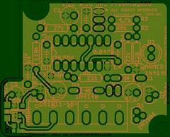
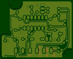
The PCB is designed as a two layer PCB with through-hole parts on the top layer to enable those less skilled with a soldering iron to build the circuit.

FreePlay 555 Fab A Top Layer w/ Silkscreen

FreePlay 555 Fab A Bottom w/ Silkscreen
For those without PCB layout tools; a bare PCB is available from the batchpcb service for under $14. You can purchase the boards from this link:
http://batchpcb.com/index.php/Products/75967
The Bill Of Materials (BOM) of the board is available from Digikey for $9.02 (as of the time of this post). A bom is included with the schematics PDF above, but An XLS file with the digikey part numbers with the complete package of the materials above as a single download: FreePlay555_pkg
The author’s prototype was built from mostly RadioShack parts he had in his parts bin including the breadboard. He intends to replace this with a PCB from batchpcb in a few months.
Installation note: You need to make sure this circuit used the same voltage rail of your cpu board. The authors’ G08 wiring harnesses did not follow either the Cockpit (which is correct) schematics or the Upright harness (which is incorrect). The J4/P5/p12 harness shows that the cockpit connects the coindoor lamps to the +5V rail at P5 pin6 and pin8. However, The author’s harness had it connected to the -5V rail which is BAD and will prevent the circuit from working properly (and possibly damaging your machine). The upright schematic shows that +5 and -5V goes to the lamps for 10V… also bad.
Either wire up a new +5V signal to this board; or correct your wiring harness to be like the schematics of the cockpit. Seriously – go double check it.
I wired in this circuit into the coin door harness so the board can be bolted to the inside the door. You’ll need to “cut” the NC wire of one of your coin switchs and put this circuit between it at J2-5 and J2-6. Then wire in the NO signal at J2-4. The Start Button goes to J2-3, the +5V rail to J2-1, and Ground to J2-2.
The circuit works as expected in my machine…. providing an inital “Free” credit upon powerup and then providing additional credits each time the start button is pressed (after the game starts). If you want more than one credit; the circuit can be redesigned; or you can press start multiple times during your “inital” game. 😉
I’m fairly sure this circuit can be adapted to any arcade machine. I provided a bridge rectifier stuffing option at B1 to enable “AC” voltage inputs from 6.3V AC. Or Jp2 can be “bridged” with solder to enable 5V to via the D3 shottkey diode. I plan to test this circuit on my Bally Star Trek Pin once I get the PCBs back.
Enjoy… I’ll post more pictures when I get the PCBs back from batchpcb.

Nice job! I chose the 8bit Atmel route, because it eliminated all of the passive components. One of the features of the AVR is that it features internal pullups on each pin as well as open-collector outputs.
http://www.onecircuit.com/node/41
When I initially thought about the circuit; I was going to do the AVR route… but the 555 timer is an oldskool way of doing it. Cheap too. I like that you can get everything from radioshack except the reset device.
I also toyed with the idea of just buying your onecircuit device; however, it wasn’t clear how it’d work with the Sega Star Trek flip-flop mechanism.
Hey,
Great bit of work you’ve put together here. Enjoyed the step by step guide. Do you have an email I can grab you on? I have a few questions Id ideally like to fire your way. Thanks
Ryan
Ryan,
You can reach me at zittware AT hotmail DOT com
while I work on a more elegant solution for the blog site.
However, if the question are on-topic; please use this comment section.
Thanks for the awesome project. The batchpcb link is redirected to the OSH Park website and it doesn’t appear that they have your board design. Do you have a new link or perhaps could I get the Gerbers?
Correct. OSHPark took over from BatchPCB and the designs were not transferred.
Give me a couple of days to look thru my designs and see if I can upload the design to OSHPark.