Over the past couple of weeks; I’ve been designing a replacement G80 PSU for the Sega/Gremlin G80 Vector machines specifically for my Star Trek Captain’s Chair.
I began by using National’s WebBench to design a simulate the 5V and 12V switching PSUs which would replace the linear PSUs on the original board. IMHO; the problem with existing linears is that you’re limited to the Pd of the BJT in the circuit. That BJT leads to a lot of wasted heat in the system. Having said that; I like linear supplies as they are easy to debug and build… for less than 1A of draw.
The Transformer and diode bidges will remain. My intent it to have the board somewhat drop in place of the existing board. I say somewhat; because the power-MOSFETs will need to be bolted to the existing heat sink on both switchers. I’ll probably keep the linears for the negative rails.
I imagine one will have to drill and tap the existing heatsink with some new mounting holes for the mosfets.
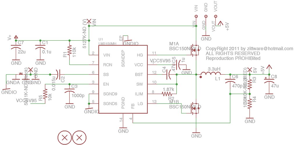
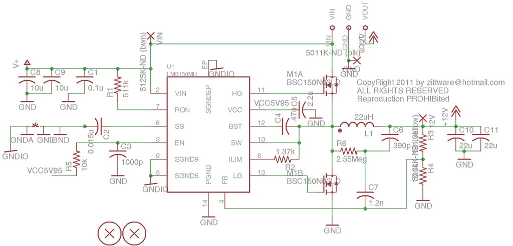
Web-bench gave me the following designs:

These boards were laid out and put on a single piece of FR4 so they can be assembled as a pair. The design is currently in my BatchPCB shopping cart; waiting for the parent board to complete it’s design phase. Nothing really to write home with regarding these PCBs… I expect the 5V switcher to meet a minimum of 5A… possibly much higher. It’ll likely be limited by the 8A diode bridge on the main parent board. The 12V switcher should meet a min of 2A… probably limited by the 4A bridge on the parent board.
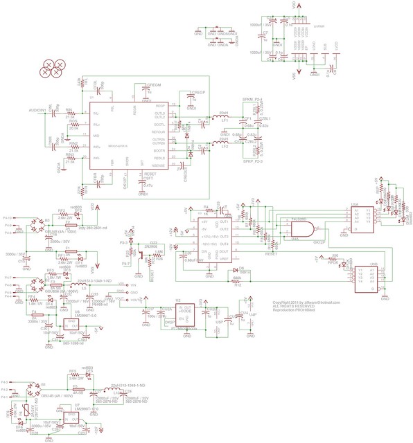
The main parent board is the host for the switching board pairs; and holds the audio amp(s). The main board is currently in development; I’m adding the 12V diode bridge and the final audio AMP.

Clearly this is an eye-chart schematic. It might be easier to look at the segaSTpsu_rev-99 .
The first notable change is that I’ve replaced the main Audio AMP #1 with a ClassD part from Maxim: MAX9742. This integrated AMP IC should provide specs better than the original discreet amp on the board. It’s configured as a bridge tied load (BTL) targeted for a 23V/V gain with a -3dB frequency of 25Hz. This -3dB frequency and gain was obtained from a spice simulation of the original discreet circuit.
Other notable changes include:
- Q23 (2N3906) makes “pull down” pulse remover for the CPU board. In the G80 PSU; R23 and D1 make up a pulse circuit which is sent to the CPU board. The CPU board has a 555 timer which implement a missing pulse detector. If a pulse is missed; it puts the CPU into reset. If my theory holds; the 2N3906 acts as a pull down preventing pulses from reaching the 555 timer – which puts the cpu in reset. So if my switching PSUs are not in regulation; this transistor effectively provides a not-“power good” signal to the CPU.
- U3, U4, and U5 are power good circuits / detectors. U3 is a MAX8215 which monitors the 4 main digital rails to the G80 card cage: +5, -5, +12V, and -12V. These four voltages are “compared” and if in regulation a high is placed on the OUTx lines. These four signals are ANDed together and sent to DIN where it’s “delayed” by ~200mS via C20/R12. This allows the PSUs to stabilize before the CPU is given the “OK” via Q23. U5A and U5B/A1 provide “power good” LEDs for the various power rails – to aid in quick debug of the G80 PSU.
- U2 provide a local 3.3V linear PSU to power U5 and the pullup on OUT3 (+12V m0nitor). This was done to enable OK12P to drive !SHDN on the ClassD amp. !SHDN cannot have more than +4V driven into it – hence the 3.3V source/pullup. Idea is to prevent premature popping/clicking while the PSU(s) are coming up. The 12V should take the longest to come in regulation and it’s also similar to the VDD/VSS supplies used in the ClassD amp. Additionally !RESET (Dout/U3) drives the “mute” pin of the (SFT / U1) meaning the ClassD amp should remain muted until the “power good” signal is sent to the cpu board.
- C32/33/L5 (and C27/24/L12) provide a PI filter to reduce vripple into the switching regulators- increasing their stability.
- I kept Linear Regulators for the lower power rails (-5 and -12) but upgraded the regulators to the National LM2990 as they provide better short circuit protection and slightly more current (1.8A). If desired; one could “in theory” drop in the cheaper/older 79xx series negative regulators to save costs. They are pin compatible.
- I’ve put fuses on the +/-12V regulator inputs which are missing from the original G80 design. F6 is a resettable fuse given it’s low power and we need board real estate for other items.
- Finally LEDs were put in parallel and under the glass fuses on the board. The theory is that if a fuse blows; the LED become a small 10ma current path and the LED lights indicating to the user that the fuse is blown. I neat debug feature if you ask me -hope it works.
I hope to complete the main board design as soon as my upgraded pcb license comes in.
Once I finish the design and validate/test it… I plan to release the design and PCBs via the TAPR open source license.
See a design error? Speak up!
