As seen in the Worklogs for the Star Trek: Mirror Universe Pinball project; Making custom shaped PCBs in EagleCad isn’t all that difficult. With a CAD file; one can make some pretty unique shapes to fit the project you’re working on. This tutorial aims to show just how easy it to create the perfect shaped PCB. The Author used this technique to create custom LED boards in the Mirror Universe project which replaced all the Switched Illumination sockets on the underside of the Playfield.
Pre-Requisites:
- EagleCad 5.11 or higher (tutorial written for 5.11).
- DXF2SCR from micromagic systems. (It’s Free and Awesome)
- A DXF file to convert. Scroll down for a .ZIP file containing files used in this Tutorial.
- About 10 minutes to do your first PCB outline.
Making the PCB shape
Please click the pictures below to be taken to a higher rez screen capture/picture.
1) The toughest part of this tutorial is creating the CAD file (DXF) which will serve as an input to the DXF2SCR tool. The author uses the Free GPLed version of QCAD to create DXF files. Teaching QCAD is beyond the scope of this document; but the basic principle is that you want to create the outline of the PCB in CAD via a series of curves or lines. Make sure you put in any mounting holes you want … and maybe even some documentation layers; like a center line or critical component locations. This allows your PCB to be “exact” without having to move holes, lines, or arcs in EagleCad.
Once you have the CAD (DXF) file; you can proceed to covert the file using the DXF2SCR tool. Start by opening the tool and selecting the input DXF file and the output .scr file. The SCR file is used later to “draw” on a blank PCB canvas. More on that in a bit. Make sure you match the units in which you created the DXF file. In my case; I almost always use inches. At this point I basically leave everything else at defaults of 1mil (0.001 inches) line widths and no offset. I leave the line with at 1mil because I can change the width in eaglecad based upon whatever I’m trying to accomplish. For much of the file; it’ll be an outline – and most people recommend you leave the outline as a “hairline” so the fab house doesn’t “charge” you for the additional 8mil width of the outline. Once you have the setup complete; click the Convert button on the left.
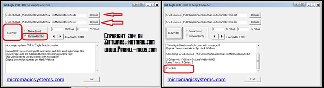
If the conversion is successful; you should see the number of lines, arcs, circles, converted along with a Complete message. If you get that, you can move on to the next step.
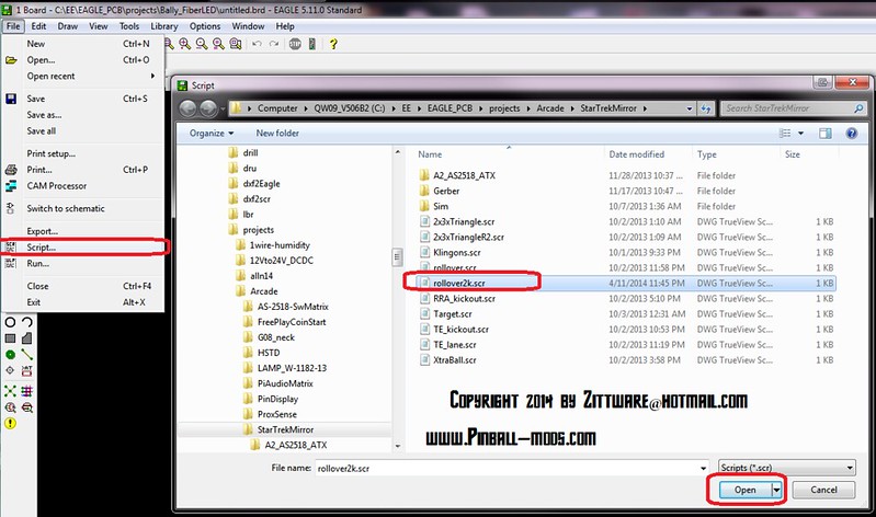
2) I start by opening EagleCad and Selecting File/New/Board… This gives me a blank canvas to create the outline on. I’m fairly sure I’ve done this on an already created board; you just have to be careful how you move the outlines and such with components are in the way. By far tho; it’s easiest that you either create the Schematic after the PCB outline, or at least make sure you don’t place parts “inside” the normal rectangle when creating the PCB from schematic.
You need to run the script created in step 1 above. This is done from the File / Script… dialog. Select the SCR you created in step 1 (or in our case rollover2k.scr) and hit open.
3)At this point EagleCad should begin executing the script drawing your arcs/lines/circles on the Dimension layer (layer 20).
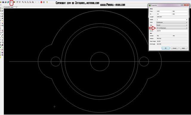
At this point you should begin to move the documentation shapes to either tDoc or bDoc and then later move them to tSilk / bSilk if necessary. You want to leave the outline and any mounting holes as 20 Dimension Layer… as that is what the gerber generator uses to generate the .oln file when you commit this design to the PCB Fab houses like OSHPark.
If you do transfer some of the lines to a silkscreen layer or even a copper layer; you should remember to change it’s width to the minimum tolerance allowed by your FAB house. In the case of a 2layer OSHPark file… it’s probably 8mils (0.008 inch).
With the steps outline above; you can basically use the CAD file as an input to even align LEDs on a evenly spaced spoke pattern or really any desirable orientation.
I’m providing the input files here for you to follow along with the steps above. Download it here:
Shaped PCB Tutorial Files
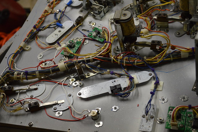
This PCB outline was used in the Star Trek: Mirror Universe as the GI lighting for the Star Rollovers. The star plunger fits inside the center hole and the two holes on the side provide mounting to the underside of the playfield. These PCBs light the Rollover from the underside with Red LEDs.

Hope this tutorial helps!
John